- 您现在的位置:买卖IC网 > Sheet目录214 > CM1224-02SR (ON Semiconductor)TVS ARRAY ESD LOW 2CH SOT143-4
CM1224
APPLICATION INFORMATION
Design Considerations
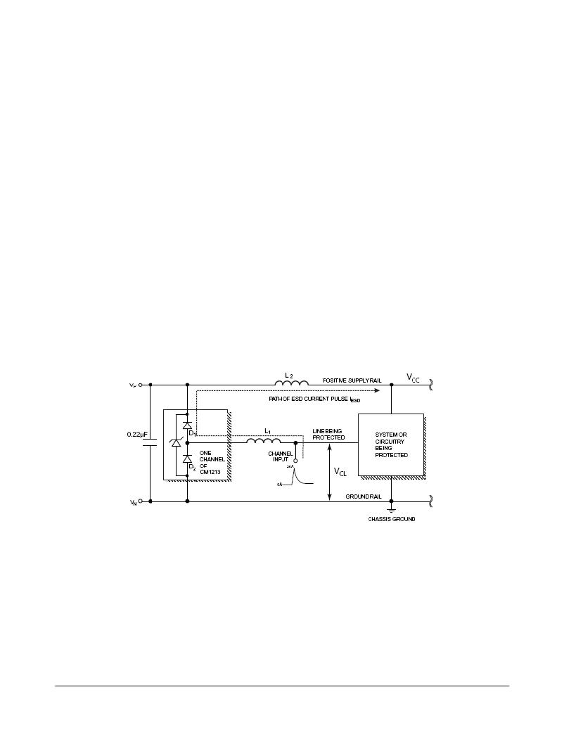
To realize the maximum protection against ESD pulses, care must be taken in the PCB layout to minimize parasitic series
inductances on the Supply/ Ground rails as well as the signal trace segment between the signal input (typically a connector)
and the ESD protection device. Figure 3 illustrates an example of a positive ESD pulse striking an input channel. The parasitic
series inductance back to the power supply is represented by L 1 and L 2 . The voltage V CL on the line being protected is:
V CL = Fwd voltage drop of D 1 + V SUPPLY + L 1 x d(I ESD ) / dt + L 2 x d(I ESD ) / dt
where I ESD is the ESD current pulse, and V SUPPLY is the positive supply voltage.
An ESD current pulse can rise from zero to its peak value in a very short time. As an example, a level 4 contact discharge
per the IEC61000 ? 4 ? 2 standard results in a current pulse that rises from 0 to 30 Amps in 1ns. Here d(I ESD )/dt can be
approximated by Δ I ESD / Δ t, or 30/(1x10 ? 9 ). So just 10 nH of series inductance (L 1 and L 2 combined) will lead to a 300 V
increment in V CL !
Similarly for negative ESD pulses, parasitic series inductance from the V N pin to the ground rail will lead to drastically
increased negative voltage on the line being protected.
The CM1224 has an integrated Zener diode between V P and V N . This greatly reduces the effect of supply rail inductance
L 2 on V CL by clamping V P at the breakdown voltage of the Zener diode. However, for the lowest possible V CL , especially when
V P is biased at a voltage significantly below the Zener breakdown voltage, it is recommended that a 0.22 m F ceramic chip
capacitor be connected between V P and the ground plane.
As a general rule, the ESD Protection Array should be located as close as possible to the point of entry of expected
electrostatic discharges. The power supply bypass capacitor mentioned earlier should be as close to the V P pin of the Protection
Array as possible, with minimum PCB trace lengths to the power supply, ground planes and between the signal input and the
ESD device to minimize stray series inductance.
Additional Information
See also ON Semiconductor Application Note “Design Considerations for ESD Protection”.
Figure 3. Application of Positive ESD Pulse between Input Channel and Ground
http://onsemi.com
6
发布紧急采购,3分钟左右您将得到回复。
相关PDF资料
CM1225-04DE
TVS ARRAY ESD LOW PROT 4CH 10DFN
CM1230-04CP
TVS ARRAY ESD LOW PROT 4CH CSP6
CM1231-02SO
DIODE ESD CLAMP 2CH SOT23-6
CM1233-08DE
DIODE ESD CLAMP ARRAY 8CH 16WDFN
CM1234-08DE
IC ESD PROTECT ARRAY HS 16TDFN
CM1235-08DE
DIODE ESD CLAMP ARRAY 8CH 16WDFN
CM1236-08DE
ARRAY ESD PROT HI SPD 8CH 16TDFN
CM1241-04D4
IC ESD PROT ARRAY ESD LOCAP 8DFN
相关代理商/技术参数
CM1224-04MR
功能描述:ESD 抑制器 4-ch. 0.7pF Ultra Lo RoHS:否 制造商:STMicroelectronics 通道:8 Channels 击穿电压:8 V 电容:45 pF 端接类型:SMD/SMT 封装 / 箱体:uQFN-16 功率耗散 Pd: 工作温度范围:- 40 C to + 85 C
CM1224-04SO
功能描述:ESD 抑制器 4-ch. 0.7pF Ultra Lo RoHS:否 制造商:STMicroelectronics 通道:8 Channels 击穿电压:8 V 电容:45 pF 端接类型:SMD/SMT 封装 / 箱体:uQFN-16 功率耗散 Pd: 工作温度范围:- 40 C to + 85 C
CM1224K
制造商:CML 制造商全称:Chicago Miniature Lamp,inc 功能描述:R-12 Single Contact Bayonet Base
CM1225
制造商:ONSEMI 制造商全称:ON Semiconductor 功能描述:4-Channel Low Capacitance ESD Protection Arrays
CM-1225
功能描述:机架和机柜配件 1.75"X19" CBL/PANEL
RoHS:否 制造商:Bivar 产品:Rack Accessories 面板空间: 颜色:Black
CM1225-04DE
功能描述:ESD 抑制器 4-ch ESD Protection 0.7pF Capacitance RoHS:否 制造商:STMicroelectronics 通道:8 Channels 击穿电压:8 V 电容:45 pF 端接类型:SMD/SMT 封装 / 箱体:uQFN-16 功率耗散 Pd: 工作温度范围:- 40 C to + 85 C
CM1226-04DE
功能描述:ESD 抑制器 4-ch ESD Protection 0.7pF Capacitance RoHS:否 制造商:STMicroelectronics 通道:8 Channels 击穿电压:8 V 电容:45 pF 端接类型:SMD/SMT 封装 / 箱体:uQFN-16 功率耗散 Pd: 工作温度范围:- 40 C to + 85 C
CM-1227
功能描述:机架和机柜配件 3.5"X19" CBL/PANEL
RoHS:否 制造商:Bivar 产品:Rack Accessories 面板空间: 颜色:Black
